Previous Chapter:500 ohm resistor 500 ohm resistor color code
Next Chapter:What is Embedded Processors and Controllers
What is the structure and function of PCB?

Post Date:2024-05-16,AMD
What is the structure and function of PCB?
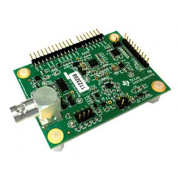
PCB (Printed Circuit Board) is one of the basic components in modern electronic equipment. It provides a platform to support and connect electronic components.
The structure of PCB mainly includes the following parts:
1. Substrate application characteristics: The basic structure of PCB is usually composed of a non-conductive material, such as fiberglass-reinforced epoxy resin (FR-4), aluminum substrate, or multi-layer thin plastic. This material provides the structural support and insulation functions of the PCB.
FR-4
Description: One of the most common substrates, consisting of woven fiberglass cloth impregnated with epoxy resin.
Characteristics: Good mechanical strength, high electrical insulation, and high cost performance.
Applications: Widely used in various industries due to its versatility and suitability for most standard PCB applications.
Aluminum base
Description: Consists of an aluminum base layer, usually coated with a dielectric layer.
Features: Excellent thermal conductivity can effectively dissipate heat, suitable for high-power applications.
Applications: Commonly used in power electronics, LED lighting and applications requiring efficient thermal management.
ceramic base
Description: Made of ceramic materials such as aluminum oxide (Al2O3) or aluminum nitride (AlN).
Features: Excellent thermal conductivity, excellent electrical insulation and high temperature stability.
Applications: Suitable for high frequency and high power applications, RF/microwave systems, and environments with extreme operating conditions.
Polyimide (PI)
Description: A flexible substrate material known for its flexibility and lightweight properties.
Features: Good chemical resistance, flexibility and thermal stability make it suitable for flexible and rigid-flex PCBs.
Applications: For applications where flexibility is critical, such as wearable electronics, aerospace and automotive industries.
Rogers Materials
Description: A brand of high frequency laminates offering different dielectric constants.
Features: Designed for high frequency applications, providing low loss and controlled impedance.
Applications: Commonly used in RF/microwave circuits, antennas and telecommunications.
Metal core (MCPCB)
Description: Uses a metal core (usually aluminum or copper) as the substrate to enhance thermal conductivity.
Features: Due to its high thermal conductivity, it enables efficient thermal management and is ideal for heat dissipation of LEDs and power electronics.
Applications: LED lighting, automotive electronics, power supplies, and applications requiring effective heat dissipation.
2. Key characteristics of Conductive Layers: PCB is covered with one or more layers of conductive material, usually copper. These copper layers are used to make circuit connections, traces, and solder joints. When manufacturing PCB, the unnecessary copper layer is removed through chemical etching or mechanical removal to form the required circuit pattern.
copper foil
Substrate: Copper is preferred due to its excellent electrical conductivity.
Thickness: Typically available in a variety of thicknesses, usually measured in ounces per square foot (oz).
Surface Treatment: Foils can have surface treatments such as ENIG (Electroless Nickel Immersion Gold) or HASL (Hot Air Solder Leveling) to enhance solderability.
layer arrangement
Single-sided PCB: A conductive layer on one side of the substrate.
Double-sided PCB: There are conductive layers on both sides of the substrate, interconnected by vias.
Multilayer PCB: Contains multiple conductive layers separated by dielectric materials and interconnected by vias to implement complex circuits.
routing and tracking
Conductive Paths: Traces are the conductive paths that connect components and form the circuit layout.
Width and Spacing: Determined by the current carrying capacity and electrical characteristics required of the circuit.
Power and ground layers
Power plane: A dedicated layer used to deliver power to components, reduce interference, and provide a low-impedance path.
Ground plane: serves as a reference point for electrical signals and minimizes noise and interference.
by connecting
Via: A connection between conductive layers through a drilled hole filled with conductive material.
Blind and buried vias: Selectively connect inner layers to optimize space in multi-layer boards.
3. Insulating Layers: There are usually insulating layers between the conductor layers and the uppermost/lowermost layer. These insulation layers are usually made of insulating materials such as epoxy or polyimide (PI) and are used to isolate different circuit layers and prevent short circuits and other circuit failures.
4. Printed Layer: The printed layer on the PCB usually includes information such as logos, text, numbers, etc. to help assembly and maintenance personnel correctly install and maintain electronic components.
Print layer purpose and function
Component Identification: Displays reference designators, part numbers, component outlines, or polarity markings for easy identification during assembly and troubleshooting.
ASSEMBLY INSTRUCTIONS: Printed indicators guide component placement and orientation to aid in accurate assembly.
Branding and Logo: Manufacturers often include their logo or brand information on the screen printing layer.
printing art
Screen Printing: Similar to the process of applying solder mask, screen printing is used to add the desired information to the PCB.
Ink type: Typically, white ink is used to contrast with the green solder mask of the circuit board, but other colors may be used depending on design requirements.
Placement and precision
Layer Location: Located on the top and/or bottom layer of the PCB, usually above the solder mask.
Accuracy: Screen printing requires precise alignment and registration to ensure the information is correctly placed relative to the features of the PCB.
5. Vias: In order to establish electrical connections between different layers, PCBs usually include through holes or vias. The holes are filled or plated with conductive material to make connections.
6. Pads: Pads are areas used to connect the pins of electronic components. They are usually located at specific locations on the PCB and match the circuit pattern. Pads can be round, square, or other shapes, depending on the component's pin design and mounting requirements.
7. Interconnections: In multi-layer PCB, the connections between layers are realized through vias and inner layer lines. These connections are precisely laid out at design time to achieve the required circuit functionality.

PCB boards are divided into single-layer boards, double-layer boards, and multi-layer boards from the layer structure.
1. Single-layer board: a circuit board with only one side plated with copper and the other side without copper plating. Typically, components are placed on the side without copper plating and are used primarily for wiring and soldering.
Single-sided PCB is the simplest form of PCB board, with only one side covered with copper foil. Single panel is suitable for simple circuits such as electronic clocks and toys. The single-panel manufacturing process is simple and low-cost, but its functions are relatively simple.
2. Double-layer board: A circuit board with copper plated on both sides, usually referring to one side as the top layer and the other side as the bottom layer. Generally, the top layer is used as the surface where components are placed, and the bottom layer is used as the soldering surface of the components.
Double-sided panels are more complex to produce than single-sided panels, but easier to manufacture than multi-layered panels. Double-sided panels are suitable for circuits of medium complexity, such as audio, television, etc. The production of double-sided panels is flexible and components can be arranged on both sides of the board.
3. Multilayer board: A circuit board containing multiple working layers. In addition to the top and bottom layers, it also includes several middle layers. Usually, the middle layer can be used as a wiring layer, signal layer, power layer, ground layer, etc. The layers are insulated from each other, and the connections between layers are usually achieved through vias.
The production of multi-layer boards is more complicated than double-sided boards, but it can improve the density and performance of circuits. Multilayer boards are suitable for high-density, high-speed, and high-frequency circuits, such as computers, mobile phones, etc. Multilayer boards can increase the number of layers as needed to improve circuit performance.
Summarize:
The internal structure of PCB is composed of multi-layer circuit board, conductive layer, insulating layer, pad, circuit layer, circuit spacing, circuit spacing, via holes, silk screen layer and solder mask layer. These components cooperate with each other to form a complete circuit board, providing reliable electrical connection and protection for the normal operation of circuit products.
PCB (Printed Circuit Board) is one of the basic components in modern electronic equipment. It provides a platform to support and connect electronic components.
The structure of PCB mainly includes the following parts:
1. Substrate application characteristics: The basic structure of PCB is usually composed of a non-conductive material, such as fiberglass-reinforced epoxy resin (FR-4), aluminum substrate, or multi-layer thin plastic. This material provides the structural support and insulation functions of the PCB.
FR-4
Description: One of the most common substrates, consisting of woven fiberglass cloth impregnated with epoxy resin.
Characteristics: Good mechanical strength, high electrical insulation, and high cost performance.
Applications: Widely used in various industries due to its versatility and suitability for most standard PCB applications.
Aluminum base
Description: Consists of an aluminum base layer, usually coated with a dielectric layer.
Features: Excellent thermal conductivity can effectively dissipate heat, suitable for high-power applications.
Applications: Commonly used in power electronics, LED lighting and applications requiring efficient thermal management.
ceramic base
Description: Made of ceramic materials such as aluminum oxide (Al2O3) or aluminum nitride (AlN).
Features: Excellent thermal conductivity, excellent electrical insulation and high temperature stability.
Applications: Suitable for high frequency and high power applications, RF/microwave systems, and environments with extreme operating conditions.
Polyimide (PI)
Description: A flexible substrate material known for its flexibility and lightweight properties.
Features: Good chemical resistance, flexibility and thermal stability make it suitable for flexible and rigid-flex PCBs.
Applications: For applications where flexibility is critical, such as wearable electronics, aerospace and automotive industries.
Rogers Materials
Description: A brand of high frequency laminates offering different dielectric constants.
Features: Designed for high frequency applications, providing low loss and controlled impedance.
Applications: Commonly used in RF/microwave circuits, antennas and telecommunications.
Metal core (MCPCB)
Description: Uses a metal core (usually aluminum or copper) as the substrate to enhance thermal conductivity.
Features: Due to its high thermal conductivity, it enables efficient thermal management and is ideal for heat dissipation of LEDs and power electronics.
Applications: LED lighting, automotive electronics, power supplies, and applications requiring effective heat dissipation.

2. Key characteristics of Conductive Layers: PCB is covered with one or more layers of conductive material, usually copper. These copper layers are used to make circuit connections, traces, and solder joints. When manufacturing PCB, the unnecessary copper layer is removed through chemical etching or mechanical removal to form the required circuit pattern.
copper foil
Substrate: Copper is preferred due to its excellent electrical conductivity.
Thickness: Typically available in a variety of thicknesses, usually measured in ounces per square foot (oz).
Surface Treatment: Foils can have surface treatments such as ENIG (Electroless Nickel Immersion Gold) or HASL (Hot Air Solder Leveling) to enhance solderability.
layer arrangement
Single-sided PCB: A conductive layer on one side of the substrate.
Double-sided PCB: There are conductive layers on both sides of the substrate, interconnected by vias.
Multilayer PCB: Contains multiple conductive layers separated by dielectric materials and interconnected by vias to implement complex circuits.
routing and tracking
Conductive Paths: Traces are the conductive paths that connect components and form the circuit layout.
Width and Spacing: Determined by the current carrying capacity and electrical characteristics required of the circuit.
Power and ground layers
Power plane: A dedicated layer used to deliver power to components, reduce interference, and provide a low-impedance path.
Ground plane: serves as a reference point for electrical signals and minimizes noise and interference.
by connecting
Via: A connection between conductive layers through a drilled hole filled with conductive material.
Blind and buried vias: Selectively connect inner layers to optimize space in multi-layer boards.

3. Insulating Layers: There are usually insulating layers between the conductor layers and the uppermost/lowermost layer. These insulation layers are usually made of insulating materials such as epoxy or polyimide (PI) and are used to isolate different circuit layers and prevent short circuits and other circuit failures.
4. Printed Layer: The printed layer on the PCB usually includes information such as logos, text, numbers, etc. to help assembly and maintenance personnel correctly install and maintain electronic components.
Print layer purpose and function
Component Identification: Displays reference designators, part numbers, component outlines, or polarity markings for easy identification during assembly and troubleshooting.
ASSEMBLY INSTRUCTIONS: Printed indicators guide component placement and orientation to aid in accurate assembly.
Branding and Logo: Manufacturers often include their logo or brand information on the screen printing layer.
printing art
Screen Printing: Similar to the process of applying solder mask, screen printing is used to add the desired information to the PCB.
Ink type: Typically, white ink is used to contrast with the green solder mask of the circuit board, but other colors may be used depending on design requirements.
Placement and precision
Layer Location: Located on the top and/or bottom layer of the PCB, usually above the solder mask.
Accuracy: Screen printing requires precise alignment and registration to ensure the information is correctly placed relative to the features of the PCB.
5. Vias: In order to establish electrical connections between different layers, PCBs usually include through holes or vias. The holes are filled or plated with conductive material to make connections.
6. Pads: Pads are areas used to connect the pins of electronic components. They are usually located at specific locations on the PCB and match the circuit pattern. Pads can be round, square, or other shapes, depending on the component's pin design and mounting requirements.
7. Interconnections: In multi-layer PCB, the connections between layers are realized through vias and inner layer lines. These connections are precisely laid out at design time to achieve the required circuit functionality.

PCB boards are divided into single-layer boards, double-layer boards, and multi-layer boards from the layer structure.
1. Single-layer board: a circuit board with only one side plated with copper and the other side without copper plating. Typically, components are placed on the side without copper plating and are used primarily for wiring and soldering.
Single-sided PCB is the simplest form of PCB board, with only one side covered with copper foil. Single panel is suitable for simple circuits such as electronic clocks and toys. The single-panel manufacturing process is simple and low-cost, but its functions are relatively simple.
2. Double-layer board: A circuit board with copper plated on both sides, usually referring to one side as the top layer and the other side as the bottom layer. Generally, the top layer is used as the surface where components are placed, and the bottom layer is used as the soldering surface of the components.
Double-sided panels are more complex to produce than single-sided panels, but easier to manufacture than multi-layered panels. Double-sided panels are suitable for circuits of medium complexity, such as audio, television, etc. The production of double-sided panels is flexible and components can be arranged on both sides of the board.
3. Multilayer board: A circuit board containing multiple working layers. In addition to the top and bottom layers, it also includes several middle layers. Usually, the middle layer can be used as a wiring layer, signal layer, power layer, ground layer, etc. The layers are insulated from each other, and the connections between layers are usually achieved through vias.
The production of multi-layer boards is more complicated than double-sided boards, but it can improve the density and performance of circuits. Multilayer boards are suitable for high-density, high-speed, and high-frequency circuits, such as computers, mobile phones, etc. Multilayer boards can increase the number of layers as needed to improve circuit performance.
Summarize:
The internal structure of PCB is composed of multi-layer circuit board, conductive layer, insulating layer, pad, circuit layer, circuit spacing, circuit spacing, via holes, silk screen layer and solder mask layer. These components cooperate with each other to form a complete circuit board, providing reliable electrical connection and protection for the normal operation of circuit products.
Through these components, PCB provides a stable platform for mounting, connecting and supporting various electronic components to form a complete circuit system. With the development of technology, the structure of PCB is also constantly innovating and improving, with performance and reliability requirements.
Previous Chapter:500 ohm resistor 500 ohm resistor color code
Next Chapter:What is Embedded Processors and Controllers


